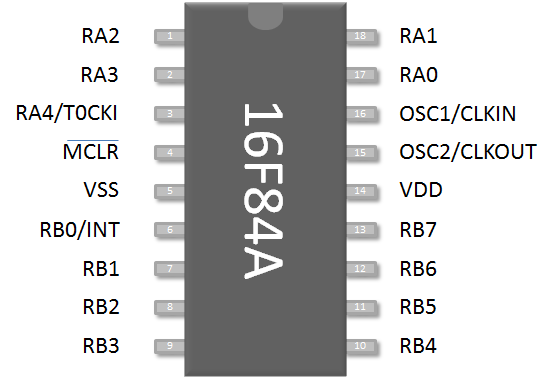
14
|
VDD |
Power Connection. Connect to +5V |
5
|
VSS |
Ground Connection |
4
|
MCLR |
Master Clear- Reset Pin.
- Logic 0 resets microcontroller.
- For proper operation connect this pin to 5V,
- NEVER keep this pin unconnected!
|
16
|
OSC1/CLKIN |
Oscillator Pin 1.
- External clock source is connected here.
- If a crystal is being used, one terminal of the crystal has to be connected to this pin, connect two 22 pF capacitors between the ground and crystal terminals
|
15
|
OSC2/CLKOUT |
Oscillator Pin 2.
- If an external clock is connected to pin 16, a square wave can be obtained here with 1/4 of the frequency supplied
- If a crystal is being used, the other terminal of the crystal has to be connected to this pin
|
17
|
RA0 |
PORTA bit 0 |
18
|
RA1 |
PORTA bit 1 |
1
|
RA2 |
PORTA bit 2 |
2
|
RA3 |
PORTA bit 3 |
3
|
RA4/T0CKI |
- RA4: PORTA bit 4
- T0CKI: Timer 0 external clock source (In order to activate, set OPTION Register-Bit 5. Option Register-Bit 4 determines the edge type for each increment)
|
6
|
RB0/INT |
- RB0: PORTB bit 0
- INT: External Interrupt (In order to activate, set INTCON Register-Bit 7 and 4. Option Register-Bit 6 determines the edge type triggerring interrupt)
|
7
|
RB1 |
PORTB bit 1 |
8
|
RB2 |
PORTB bit 2 |
9
|
RB3 |
PORTB bit 3 |
10
|
RB4 |
PORTB bit 4 |
11
|
RB5 |
PORTB bit 5 |
12
|
RB6 |
PORTB bit 6 |
13
|
RB7 |
PORTB bit 7 |